This is the seventh in a series of posts on my ESP8266 microcontroller experiences, but this time taking a more hardware bent.
In the past, I have been using a white ESP8266 (ESP12) adapter (pictured) that lets me plug an ESP12 into a breadboard. While the parts that I received did indeed fit into a breadboard, there was a flaw that I didn’t see coming - the adapter took the entire width of the breadboard, leaving no room to connect any wires to make a circuit!
I managed to get things going by finding the one breadboard that I own that just happened to have two next to each other that had the centre +/- rails narrow enough for the module to just fit across the two boards. And by “just”, I mean “having to bend the pins out half a hole’s width to make it fit.” That didn’t seem like a very good solution, especially as it mean that all ESP8266 work had to be performed on the one breadboard. This led me to try and create my own breakout board for the ESP12 module, one that is truly breadboard friendly.
What is a breakout?
So, what is a breakout board? Put simply, it’s a PCB that is used to make it easy to access the electrical contacts of a device.
A breadboard has a series of holes with a 0.1” (2.54mm) spacing, from the centre of one hole to the next in both directions. In the past, all components either had leads (like resistors, diodes, LEDs etc), or came in a DIP (Dual In-line Package) format, with 0.1” spacing - perfect for a breadboard. These days, with SMDs (surface mount devices) becoming much more common, it is getting harder to prototype things on a breadboard.
The ESP12’s connectors come with a 2mm spacing, an increasingly common standard in a metric dominated world. This, of course, means that it can’t be plugged into a breadboard, so we need a circuit board that breaks the ESP12 connectors out into a 0.1” pitch to make it suitable.
The term “breakout board” typically means simply making the pins more accessible, but there are instances where some extra components are warranted. An example of this could be the addition of crystals, resistors, capacitors and the like that are essential to chip’s operation can belong on a breakout.
When you look at boards like the Node MCU board, there’s the ESP12 module, a USB serial converter, flash/reset switches and associated circuitry. There’s a lot more going on than simply breaking out the ESP12 connections, so is it a breakout board? I’d say not, but when a simple breakout board becomes something more like a Node MCU is possibly something that different people will never agree on.
Goals
When designing a breakout board, the first question is always: “what do I want it to do?” My goals for the breakout were:
- Accept an ESP12/ESP12E/ESP12F module
- Make it fit on a standard breadboard with one set of pins to spare on each side
- Add all required pull up/down resistors to make the ESP “self-sufficient”
- Do not add any power regulation or USB interface circuitry
- Do not add reset/flash switches, they can be added externally if required
- Keep it as small as reasonably possible
- Do not route the ESP12E/ESP12F additional contacts, as they’re already used for the flash memory
The Design
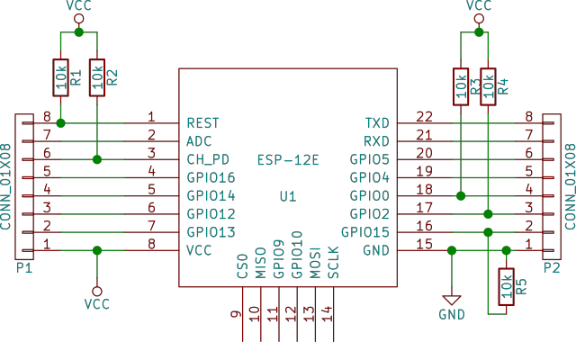
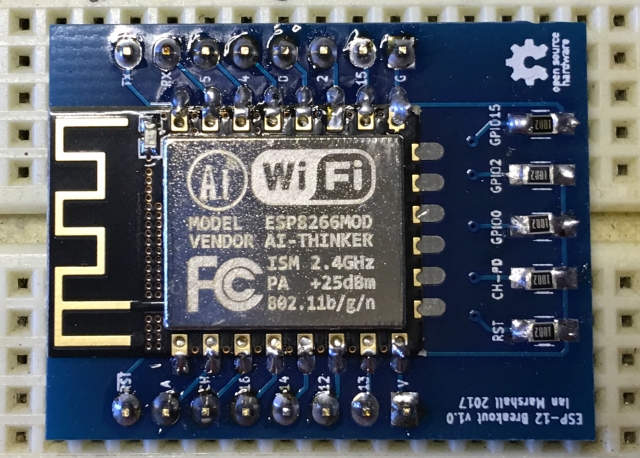
Like most other breakout boards, the schematic is very simple. I have included the five pull up/down resistors to keep the ESP8266 stable.
The schematic itself was developed in the excellent KiCad software. This is free/open source software which I highly recommend for electronics design. It is available for multiple platforms (including the Linux which I personally use) and gaining features at a rate of knots. I’ll admit that it isn’t the easiest package to get started with, but it is well worth the investment of your time. A good starter article is on Hackaday.
The Board
When designing the board, I had to be careful of the width that I was planning on having. The ESP12 module is not narrow to start with, so I had to place the pins for the breadboard second. I chose SMD resistors, as they take up far less space than the through-hole ones. I chose 0805 sized devices, as they’re large enough to hand solder. The special footprint for 0805 hand soldering in KiCad made it nice and easy.
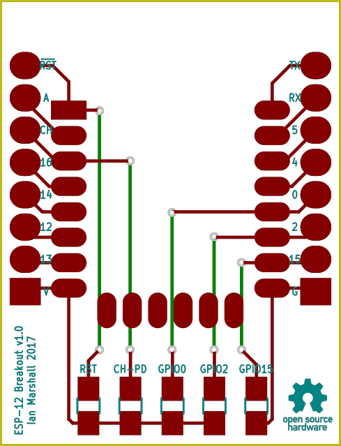
If you look closely at the board design picture, you can see that I’ve created it as a two layer board. I could probably have gotten away with a single layer by squeezing them in between the other pads, but as two layer isn’t any extra from most board makers, I thought I might as well use it.
As there is very little space between the pads for the ESP12 and those for the breadboard connections, there wasn’t a nice amount of space available for labelling the pins. In the end, I had to put just the GPIO number, or a one or two letter abbreviation as the text. This does make it harder to read, but that’s the cost of making it so thin.
The logo on the bottom right of the board is the open source hardware logo. This is used to signify that the hardware designs are all open sourced, and others can take it and build from there. The KiCad designs and resulting Gerber output (which can be sent directly to a PCB manufacturer) is available in this GitHub repository. Feel free to take these designs and build your own, or improve on it, too! If you do improve on it, please let me know - I’d love to improve my PCB designing skills.
The Result
I sent the Gerber design to Seeed Studio for manufacture, and they sent back ten shiny blue/silver boards - my first ever commercially manufactured PCBs!
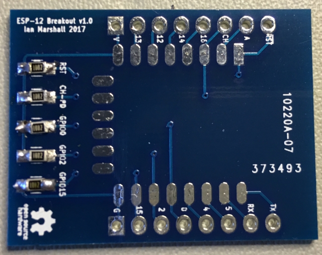
I soldered in some SMD resistors before taking the above photograph - these were actually the first ever SMDs that I’d soldered. Electrically, they all work just fine.
The final constructed PCB, with an ESP12F module soldered in, and plugged into a breadboard looks like there isn’t sufficient space for a wire to be plugged in next to it, but there actually is - just.
I have tested the breakout board in my breadboard, and successfully programmed and executed ESP8266 programs on it. I found that not having to worry about getting all of the resistors in the right locations make it a lot more fun for me to just use the ESP8266. Whether that’s actually from the breakout itself, or the satisfaction of knowing that it’s one that I designed myself, I’ll leave as an exercise for the reader to decide.
Future Changes
For my first PCB manufactured, and first ESP8266 breakout, I’m very happy with the way that it’s turned out. That said, it’s not perfect. My wish list for future possible changes are:
- Look into adding reset and flash buttons - I’d have to find some nice and very small SMD buttons for it to fit
- Make the board a little bit narrower again. The wires wouldn’t be quite so tight a fit if I shaved a bit more width off of the edge cuts
- Remove the connectors on the bottom edge of the ESP12 module - they’re not connected, so why have them? Or should I break them out?